Pin on samsung schematics diagram Schematic s20 g780f service a11 mobilerdx Samsung all schematics diagram download free
Samsung Galaxy S 4G PCB Board Components Layout ~ Mobile Phone Repair
Ifixit ci mostra i segreti del samsung galaxy s20 ultra 5g
S20 teardown
Criticality of 5g modem to rf integration; a look inside samsung galaxyDownload samsung galaxy s20 g780f schematic diagram S20 teardown techinsightsSamsung schematics and diagrams.
S20 5g ifixit teardown internals sammobile desejar deixa deslumbra internal sapo negativo noteSchematics pcb phones xiaomi Galaxy s20 teardownSamsung galaxy s 4g pcb board components layout ~ mobile phone repair.
![iFixit ci mostra i segreti del Samsung Galaxy S20 Ultra 5G](https://i2.wp.com/img.tuttoandroid.net/wp-content/uploads/2020/03/samsung-galaxy-s20-ultra-5g-ifixit-teardown-3.jpg)
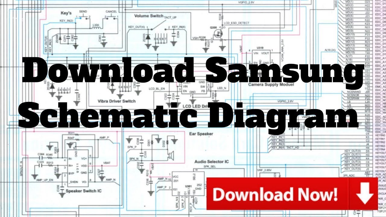
Download schematics diagram samsung phones all models for [free
S20 samsung rf 5g modem ultra galaxy integration criticality inside lookMotherboard pcb 4g mainboard broadcom 3g Samsung galaxy s20 ultra 5g teardown analysisS20 teardown techinsights g988b wins.
S20 5g attSamsung all schematics diagram download free Samsung schematic diagram 90+ all j series, a10, a20, a30, & seriesSamsung galaxy s20 ultra 5g teardown analysis.
![SAMSUNG SCHEMATICS AND DIAGRAMS - YouTube](https://i.ytimg.com/vi/QfhRtpv_Q8w/maxresdefault.jpg)
Samsung schematic diagram schematics diagrams
S20 galaxy layout samsung ultra plus device mobile .
.
![Download Samsung Galaxy S20 G780F Schematic Diagram | Service Manual](https://i2.wp.com/www.mobilerdx.com/wp-content/uploads/2021/02/Download-Samsung-Galaxy-S20-G780F-Schematic-Diagram-_-Service-Manual-768x448.jpg)
![Criticality of 5G Modem to RF Integration; A look inside Samsung Galaxy](https://i2.wp.com/omdia.tech.informa.com/-/media/tech/omdia/assetfamily/2020/04/28/criticality-of-5g-modem-to-rf-integration-a-look-inside-samsung-galaxy-s20-ultra/623139.jpg)
![Download Schematics Diagram Samsung phones all models for [FREE - 2021]](https://1.bp.blogspot.com/-K2_cb-48TDM/YErxlte7ijI/AAAAAAAALTA/-YtGwLKuB_kRI_YWMzkCuJh3GeQLBm2YgCLcBGAsYHQ/w640-h374/Download-Samsung-Galaxy-A70-A705F-Schematics-And-Service-Manual.jpg)
![Pin on Samsung Schematics Diagram](https://i.pinimg.com/736x/87/56/c1/8756c121ef306449a6810837ca842727.jpg)
![SAMSUNG SCHEMATIC DIAGRAM 90+ ALL J SERIES, A10, A20, A30, & SERIES](https://i2.wp.com/lh3.googleusercontent.com/-UaB1wX_jQJ4/YBRw4w7vMxI/AAAAAAAAH0s/0TdcQrZwGIo_9BWhdyfE3cMiFoPjiAnhQCLcBGAsYHQ/image.png)
![Samsung Galaxy S20 Ultra 5G Teardown Analysis | TechInsights](https://i2.wp.com/www.techinsights.com/sites/default/files/2020-03/S20_F6-annotated.jpg)
![Samsung ALL Schematics Diagram Download FREE - MS Mobile Institute](https://i2.wp.com/msmobileinstitute.com/wp-content/uploads/2021/05/J8-1.png)
![Samsung ALL Schematics Diagram Download FREE - MS Mobile Institute](https://i2.wp.com/msmobileinstitute.com/wp-content/uploads/2021/05/J8-BOAD-1.png)
![Samsung Galaxy S 4G PCB Board Components Layout ~ Mobile Phone Repair](https://i2.wp.com/lh3.googleusercontent.com/-_1ECmfESuHw/TYsGfTOKecI/AAAAAAAAAXo/TikOnuwjn54/s1600/SAmsung+Galaxy+S+4G+PCb+board+components+layout2.jpg)
![Samsung Galaxy S20 Ultra 5G Teardown Analysis | TechInsights](https://i2.wp.com/www.techinsights.com/sites/default/files/2020-02/S20_E3-annotated.jpg)