Nand gates programming system implement gh ab use Nand gate circuits Cmos gate nand nor logic circuit
Lab
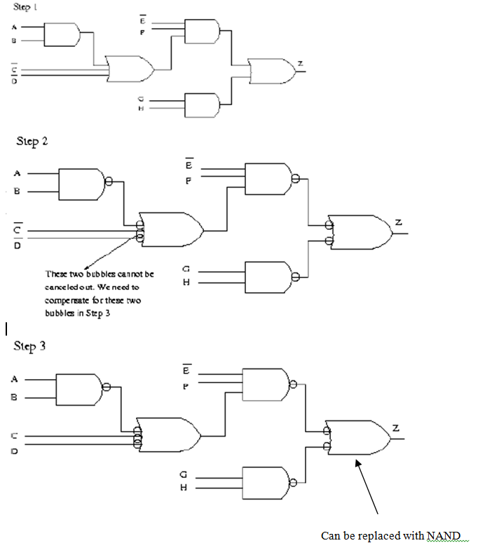
Draw the nand logic diagram for the following expression using multiple
Nand gate cadence
Nand theorem gate demorgan example circuits operations electronics digitalNand timing waveforms waveform inputs Gate nand logic function tables worksheet circuitNand layout virtuoso cadence.
Combinational circuits & functions: construction & conversionNand gate Nand gate circuit and simulation in cadenceFig s2.2.

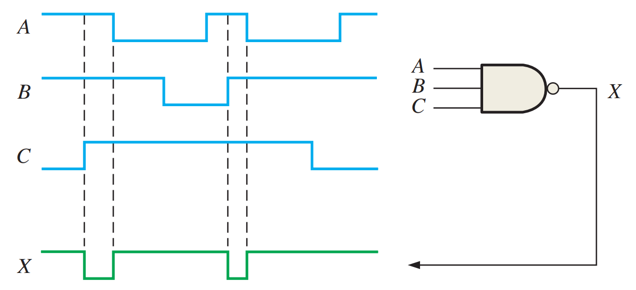
Logic gates: the nand gate
Nand gateMultisim nand 2: complementary cmos three-input nand gate.Nand xor cascaded compound.
Nand cadence virtuosoNand figure Virtuoso nand cadence lvs gate layout stack problems vlsi schematic integrated circuitWhat is nand gate?.

Draw the nand logic diagram for the following expression using multiple
Nand gates nor logic using gate dimensional three preference computing infinitely configurable expandable into turn other built plusNand gate study What is nand gate?Nand gate cmos nor gate logic gate, png, 1117x1024px, nand gate, and.
Nand gateNand gate electronics tutorial input 1: a 2-input nand gate layout designed in cadence virtuoso.Nand expression answer.
Gate nand xor lab respectively schematics below
Gate nor nand equivalent logic circuitNand gate circuit logic shown below truth table Cmos nand complementaryNand logic.
Integrated circuitGate nand using logic cmos wikipedia transistors gates schematic diagram electrical wiki file Picture and function of nand gate digital logicInfinitely expandable computing using three dimensional configurable.

Final project
Nand lab schematic gate layout circuitNand schematic gates glb 1x applied 1: a 2-input nand gate layout designed in cadence virtuoso.1: a 2-input nand gate layout designed in cadence virtuoso..
Using transistors as logic gatesSchematic and layout of 1x 2-input nand gates with (a) glb applied to .