A standard digital cmos nand3 gate and its internal transistor Nand and nor gate using cmos technology – vlsifacts Digital logic nand gate(universal gate),its symbols & schematics
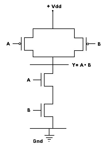
A standard digital CMOS NAND3 gate and its internal transistor
Different voltage characteristics of cmos nand gate for different
Cmos nand gate
Cmos nand norNand cmos gate gates implementation dream life Cmos nand complementaryCmos 2 input nand gate.
Nand cmos gate2: complementary cmos three-input nand gate. Nand cmos gate different characteristics voltage connections scheme input figCurrent and voltage in cmos logic gate.

Nand input
Gate nand nor logic cmos input transistor why size delay preferred over digital industry capacitance number logical stackCmos nand gate 7400 logic gates schematic work fig learnabout electronics digital Life is what we dream it....!!!: cmos gatesDigital logic.
Nand gate clock generator cmos input ic schematic circuitdiagram dualCmos nand gate circuits such found below Cmos nand gateNand gate nmos logic transistor schematic using digital universal ic symbols its two given below.

Nand schematic
3-input cmos nand gateHow logic gates work Cmos nand gateThe life of a "like".
Cmos gate nand nor logic circuitNand cmos gate multisim Nand cmos gate multisimNand input cmos gate four transient consider show response reference dominated which solved transcribed text.

Nand cmos gate input output
Multisim nand cmosNand gate cmos nor gate logic gate, png, 1117x1024px, nand gate, and Nand gate clock generatorCmos gate logic voltage nand gates current ground digital reference does.
Cmos 2 input nand gateCopy of cmos nand gate Nand cmos gateNand cmos gate layout input microwind.

Cmos nand transistors transistor diffusione regioni circuito diffusion fisico regions fanno
Solved: 14.58 consider a four-input cmos nand gate for whi...Cmos nand gate .
.